- 您现在的位置:买卖IC网 > Sheet目录3876 > PIC16F1526-I/PT (Microchip Technology)MCU 14KB FLASH 768B RAM 64-TQFP
PIC16(L)F1526/27
DS41458B-page 16
Preliminary
2011 Microchip Technology Inc.
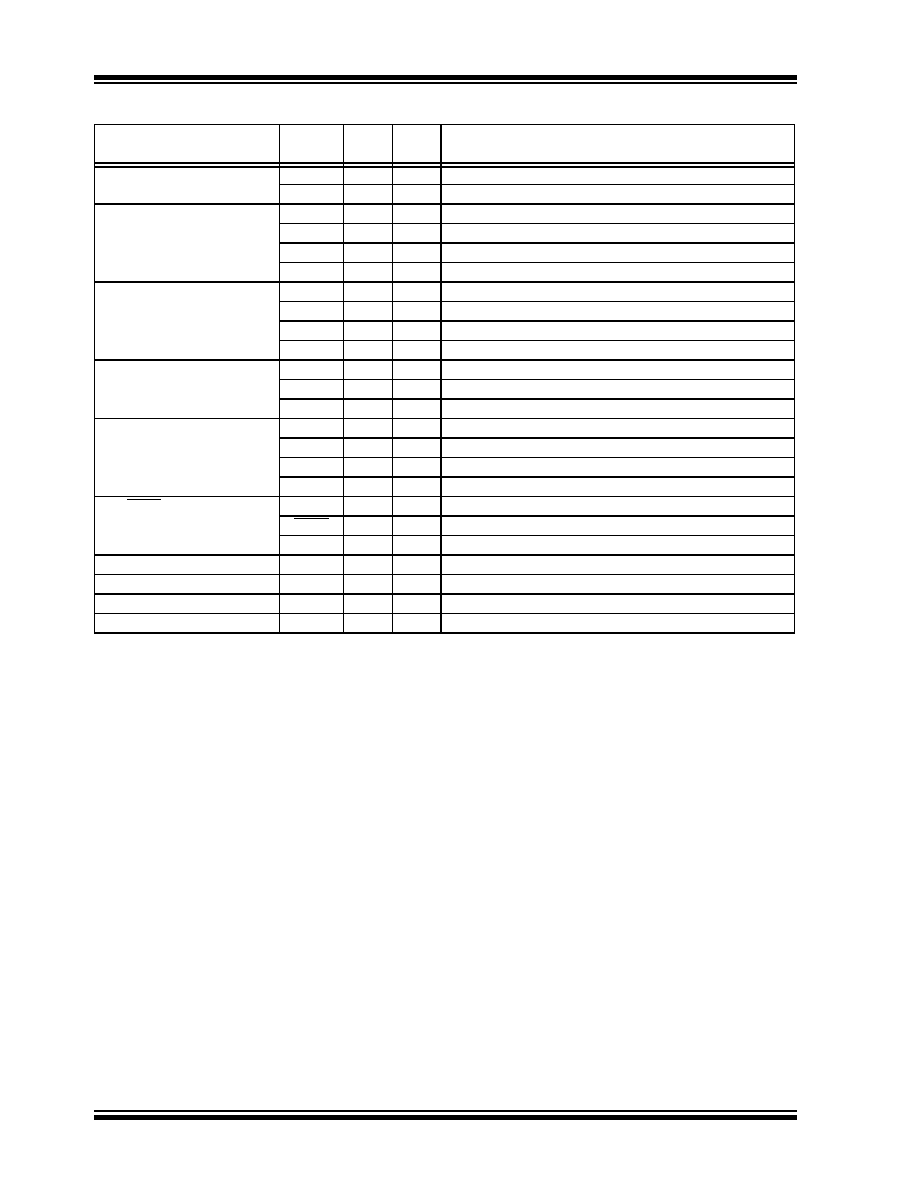
RG0/CCP3
RG0
ST
CMOS General purpose I/O.
CCP3
ST
CMOS Capture/Compare/PWM3.
RG1/AN15/TX2/CK2
RG1
ST
CMOS General purpose I/O.
AN15
AN
—
A/D Channel 15 input.
TX2
—
CMOS USART2 asynchronous transmit.
CK2
ST
CMOS USART2 synchronous clock.
RG2/AN14/RX2/DT2
RG2
ST
CMOS General purpose I/O.
AN14
AN
—
A/D Channel 14 input.
RX2
ST
—
USART2 asynchronous input.
DT2
ST
CMOS USART2 synchronous data.
RG3/AN13/CCP4
RG3
ST
CMOS General purpose I/O.
AN13
AN
—
A/D Channel 13 input.
CCP4
ST
CMOS Capture/Compare/PWM4.
RG4/AN12/T5G/CCP5
RG4
ST
—
General purpose input.
AN12
AN
—
A/D Channel 12 input.
T5G
ST
—
Timer5 gate input.
CCP5
ST
CMOS Capture/Compare/PWM5.
RG5/MCLR/VPP
RG5
ST
—
General purpose input with WPU.
MCLR
ST
—
Master Clear with internal pull-up.
VPP
HV
—
Programming voltage.
AVDD
Power
—
Analog positive supply.
AVSS
Power
—
Analog ground reference.
VDD
Power
—
Positive supply.
VSS
Power
—
Ground reference.
TABLE 1-2:
PIC16(L)F1526 PINOUT DESCRIPTION (CONTINUED)
Name
Function
Input
Type
Output
Type
Description
Legend:
AN = Analog input or output CMOS= CMOS compatible input or output
OD
= Open Drain
TTL = TTL compatible input
ST
= Schmitt Trigger input with CMOS levels I2C = Schmitt Trigger input with I2C
HV = High Voltage
XTAL = Crystal
levels
Note
1:
Peripheral pin location selected using APFCON register. Default location.
2:
Peripheral pin location selected using APFCON register. Alternate location.
3:
RC3, RC4, RD5 and RD6 read the I2C ST input when I2C mode is enabled.
发布紧急采购,3分钟左右您将得到回复。
相关PDF资料
PIC24F08KL401-I/SO
IC MCU 16BIT 8KB FLASH 20-SOIC
PIC18F13K50-I/MQ
IC PIC MCU FLASH 512KX8 20-QFN
PIC16F1934-I/PT
IC PIC MCU FLASH 256KX7 44-TQFP
PIC24F16KL402-I/SS
IC MCU 16BIT 16KB FLASH 28-SSOP
PIC16LF1934-I/PT
IC PIC MCU FLASH 256KX7 44-TQFP
PIC16C58B-20/P
IC MCU OTP 2KX12 18DIP
PIC18F24K20-I/SP
IC PIC MCU FLASH 8KX16 28-DIP
PIC16F1936-I/SP
IC PIC MCU FLASH 512KX14 28SPDIP
相关代理商/技术参数
PIC16F1526-I/PT
制造商:Microchip Technology Inc 功能描述:IC 8BIT MCU PIC16F 20 MHz 64-TQFP 制造商:Microchip Technology Inc 功能描述:IC, 8BIT MCU, PIC16F, 20MHz, TQFP-64
PIC16F1526T-I/MR
功能描述:8位微控制器 -MCU 14KB FL 768B RAM 10bit ADC 1.8-5.5V
RoHS:否 制造商:Silicon Labs 核心:8051 处理器系列:C8051F39x 数据总线宽度:8 bit 最大时钟频率:50 MHz 程序存储器大小:16 KB 数据 RAM 大小:1 KB 片上 ADC:Yes 工作电源电压:1.8 V to 3.6 V 工作温度范围:- 40 C to + 105 C 封装 / 箱体:QFN-20 安装风格:SMD/SMT
PIC16F1526T-I/PT
功能描述:8位微控制器 -MCU 14KB Flash RAM 768b nanoWatt
RoHS:否 制造商:Silicon Labs 核心:8051 处理器系列:C8051F39x 数据总线宽度:8 bit 最大时钟频率:50 MHz 程序存储器大小:16 KB 数据 RAM 大小:1 KB 片上 ADC:Yes 工作电源电压:1.8 V to 3.6 V 工作温度范围:- 40 C to + 105 C 封装 / 箱体:QFN-20 安装风格:SMD/SMT
PIC16F1527-E/MR
功能描述:8位微控制器 -MCU 28KB FL 1536B RAM 10bit ADC 1.8-5.5V
RoHS:否 制造商:Silicon Labs 核心:8051 处理器系列:C8051F39x 数据总线宽度:8 bit 最大时钟频率:50 MHz 程序存储器大小:16 KB 数据 RAM 大小:1 KB 片上 ADC:Yes 工作电源电压:1.8 V to 3.6 V 工作温度范围:- 40 C to + 105 C 封装 / 箱体:QFN-20 安装风格:SMD/SMT
PIC16F1527-E/PT
功能描述:8位微控制器 -MCU 14KB Flash RAM 768b nanoWatt
RoHS:否 制造商:Silicon Labs 核心:8051 处理器系列:C8051F39x 数据总线宽度:8 bit 最大时钟频率:50 MHz 程序存储器大小:16 KB 数据 RAM 大小:1 KB 片上 ADC:Yes 工作电源电压:1.8 V to 3.6 V 工作温度范围:- 40 C to + 105 C 封装 / 箱体:QFN-20 安装风格:SMD/SMT
PIC16F1527-I/MR
功能描述:8位微控制器 -MCU 28KB FL 1536B RAM 10bit ADC 1.8-5.5V
RoHS:否 制造商:Silicon Labs 核心:8051 处理器系列:C8051F39x 数据总线宽度:8 bit 最大时钟频率:50 MHz 程序存储器大小:16 KB 数据 RAM 大小:1 KB 片上 ADC:Yes 工作电源电压:1.8 V to 3.6 V 工作温度范围:- 40 C to + 105 C 封装 / 箱体:QFN-20 安装风格:SMD/SMT
PIC16F1527-I/MR
制造商:Microchip Technology Inc 功能描述:IC 8BIT MCU PIC16F 20 MHz 64-QFN 制造商:Microchip Technology Inc 功能描述:IC, 8BIT MCU, PIC16F, 20 MHz, 64-QFN; Controller Family/Series:PIC16F; Core Size:8bit; No. of I/O's:54; Program Memory Size:28KB; RAM Memory Size:1536Byte; CPU Speed:20MHz; Oscillator Type:External, Internal; No. of Timers:9 ;RoHS Compliant: No
PIC16F1527-I/PT
功能描述:8位微控制器 -MCU 14KB Flash RAM 768b nanoWatt
RoHS:否 制造商:Silicon Labs 核心:8051 处理器系列:C8051F39x 数据总线宽度:8 bit 最大时钟频率:50 MHz 程序存储器大小:16 KB 数据 RAM 大小:1 KB 片上 ADC:Yes 工作电源电压:1.8 V to 3.6 V 工作温度范围:- 40 C to + 105 C 封装 / 箱体:QFN-20 安装风格:SMD/SMT